Semiconductor compounds
O-Rings, Inc. FFKM (perfluorosilicone) Seals have been specially developed to offer high performance in critical semiconductor device fabrication. They are used in semicon processes such as ALD, CVD, Etch, Dry/Wet Strip and Wet Clean. O-Rings, Inc. FFKM seals are proven to provide improved performance over traditional perfluoroelastomer materials yet with 20 to 30% reduction in cost.
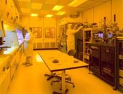
From the raw material handling to inspection and packaging, O-Rings, Inc. FFKM are processed in a cleanroom to avoid contamination which can lead to a reduction in wafer yield. High end O-Rings, Inc. FFKM seals have a unique translucent grade, and the first high-purity FFKM perfluoroelastomer material. Standard FFKM seals contain carbon or white fillers which can leach out and contaminate a process such as silicon etching. O-Rings, Inc. FFKM incorporates pure semi-crystalline, organic perfluoropolymer nano-fillers, which do not contain impurities and trace metals
| Compound | Color | Tensile Strength Mpa | Elongation Break % | 100% Modulus Mpa | Durometer Shore A | Compression Set 70hr | Max Temp |
| KB087-70 | BLACK | 11.8 | 172 | 6.36 | 70 | 27 % @200°C | 230 °C |
| KB097-70 | BLACK | 18.54 | 154 | 7.97 | 70 | 26 % @200°C | 230 °C |
| KB089-90 | BLACK | 13.73 | 121 | 13.19 | 90 | 36 % @200°C | 230 °C |
| KB099-90 | BLACK | 21.2 | 91 | 90 | 26 % @200°C | 230 °C | |
| KB025-75 | BLACK | 11.6 | 260 | 4.3 | 75 | 20 % @200°C | 250 °C |
| KB040-70 | BLACK | 19.5 | 163 | 9.3 | 70 | 18 % @200°C | 275 °C |
| KB050-70 | BLACK | 14.9 | 169 | 8.8 | 70 | 18 % @200°C | 290 °C |
| KB030-75 | BLACK | 14.7 | 177 | 9.3 | 75 | 19 % @200°C | 300 °C |
| KB055-70 | BLACK | 20 | 175 | 10.5 | 70 | 19 % @200°C | 320 °C |
| KW087-70 | WHITE | 11.86 | 173 | 5.65 | 70 | 24 % @200°C | 230 °C |
| KW097-70 | WHITE | 20.3 | 169 | 9.68 | 70 | 28 % @200°C | 230 °C |
| KW089-90 | WHITE | 15.04 | 76 | 90 | 25 % @200°C | 230 °C | |
| KW098-90 | WHITE | 22.26 | 92 | 90 | 28 % @200°C | 230 °C | |
| KW025-75 | WHITE | 11.2 | 252 | 4.8 | 75 | 32 % @200°C | 250 °C |
| KW040-70 | WHITE | 15.4 | 172 | 7.7 | 70 | 38 % @200°C | 275 °C |
| KW050-70 | WHITE | 16.7 | 193 | 13.5 | 70 | 38 % @200°C | 290 °C |
| KW030-75 | WHITE | 15.2 | 186 | 12.4 | 75 | 36 % @200°C | 300 °C |
| KW055-70 | WHITE | 19.6 | 182 | 12.3 | 70 | 36 % @200°C | 320 °C |
Semiconductor device fabrication is the process used to create chips, the integrated circuits that are present in everyday electrical and electronic devices. It is a multiple-step sequence of photographic and chemical processing steps during which electronic circuits are gradually created on a wafer made of pure semiconducting material. Silicon is the most commonly used semiconductor material today, along with gallium arsenide, germanium, and some other materials.
Wafers
A typical wafer is made out of extremely pure silicon that is grown into mono-crystalline cylindrical ingots (boules) up to 12 in (300 mm) in diameter using the Czochralski process. These ingots are then sliced into wafers about 0.75 mm thick and polished to obtain a very regular and flat surface.
Once the wafers are prepared, many process steps are necessary to produce the desired semiconductor integrated circuit. In general, the steps can be grouped into four areas:
- Front end processing
- Back end processing
- Test
- Packaging.
- Deposition is any process that grows, coats, or otherwise transfers a material onto the wafer. Available technologies consist of physical vapor deposition (PVD), chemical vapor deposition (CVD), electrochemical deposition (ECD), molecular beam epitaxy (MBE) and more recently, atomic layer deposition (ALD) among others.
- Removal processes are any that remove material from the wafer either in bulk or selective form and consist primarily of etch processes, both wet etching and dry etching such as reactive ion etch (RIE). Chemical-mechanical planarization (CMP) is also a removal process used between levels.
- Patterning covers the series of processes that shape or alter the existing shape of the deposited materials and is generally referred to as lithography. For example, in conventional lithography, the wafer is coated with a chemical called a “photoresist.” The photoresist is exposed by a “stepper”, a machine that focuses, aligns, and moves the mask, exposing select portions of the wafer to short wavelength light. The unexposed regions are washed away by a developer solution. After etching or other processing, the remaining photoresist is removed by plasma ashing.
- Modification of electrical properties has historically consisted of doping transistor sources and drains originally by diKusion furnaces and later by ion implantation. These doping processes are followed by furnace anneal or in advanced devices, by rapid thermal anneal (RTA) which serve to activate the implanted dopants. Modification of electrical properties now also extends to reduction of dielectric constant in low-k insulating materials via exposure to ultraviolet light in UV processing (UVP).
- Many modern chips have eight or more levels produced in over 300 sequenced processing steps.
- Wafer processing
- This is a list of processing techniques that are employed numerous times in a modern electronic device and do not necessarily imply a specific order.
- · Wet cleans
- · Photolithography
- · Ion implantation (in which dopants are embedded in the wafer creating regions of increased (or decreased) conductivity)
- · Dry Etching
- · Wet Etching
- · Plasma ashing
- · Thermal treatments
- · Rapid thermal anneal
- · Furnace anneals
- · Oxidation
- · Chemical vapor deposition (CVD)
- · Physical vapor deposition (PVD)
- · Molecular beam epitaxy (MBE)
- · Electrochemical Deposition (ECD). See Electroplating
- · Chemical-mechanical planarization (CMP)
- · Wafer testing (where the electrical performance is verified)
- · Wafer backgrinding (to reduce the thickness of the wafer so the resulting chip can be put into a thin device like a smartcard or PCMCIA card.)
- · Die preparation
- · Wafer mounting
- · Die cutting
- · IC packaging
- · Die attachment
- · IC Bonding
- · Wire bonding
- · Flip chip
- · Tab bonding
- · IC encapsulation
- · Baking
- · Plating
- · Lasermarking
- · Trim and form
- · IC testing
- · poisonous elemental dopants such as arsenic, boron, antimony and phosphorus
- · poisonous compounds like arsine, phosphine and silane
- · highly reactive liquids, such as hydrogen peroxide, fuming nitric acid, sulfuric acid and hydrofluoric acid
- It is vital that workers not be directly exposed to these dangerous substances. The high degree of automation common in the IC fabrication industry helps to reduce the risks of exposure of this sort.
Physical vapor deposition (PVD) is a technique used to deposit thin films of various materials onto various surfaces (e.g., of semiconductor wafers) by physical means, as compared to chemical vapor deposition.
PVD is used in the manufacture of items including semiconductor devices, aluminized PET film for balloons and snack bags, and coated cutting tools for metalworking.
Leading manufacturers of PVD tools include Applied Materials (~78.1% market share in 2004), Novellus Systems (~6.2% market share in 2004), and Oerlikon Balzers coatings (~4.8% market share in 2004). Specialty and custom PVD equipment suppliers include Platit, Metaplas Ionon, Angstrom Engineering, Johnsen Ultravac, Plasma Quest Limited, and Denton Vacuum. Leading consumers of PVD tools include Intel, Samsung, and Taiwan Semiconductor.
Variants of PVD include
- Evaporative deposition
- Sputtering
- Pulsed laser deposition
- High velocity oxygen fuel